Service

O-SiP Service

O-SiP Service
회사 이미지

About LIPAC's O-SiP Service

  • Receiving the semiconductor packaging service from OSAT* companies is not an easy
    process especially when the product is under development level, or the expected volume for mass production is not sufficient.

  • For customers who need to develop futuristic package product but cannot access to
    OSAT service, LIPAC is willing to have the partnership and deliver the satisfiable
    packaging service to the customer.

  • Upon a customer's request on exact specification and components for the package,
    LIPAC delivers full-service on package design, packaging (molding / bumping) and final
    test with highest quality and minimal delivery time.

* OSAT: Outsourced Semiconductor Assembly and Test

Process

  1. 1. Receiving spec. requirements and components from a customer

    Die information, package outline dimension, netlist and design rule should be given to LIPAC.

  2. 2. Package design

    LIPAC provides electrical and optical design service of the package. Wafer map and photo-mask design is also provided.

  3. 3. Optical / electrical IC packaging

    O-SiP fabrication based on FOWLP (Fan Out Wafer Level Package) is provided, including wafer-level molding and bumping process.

  4. 4. Final-testing the package

    Visual inspection and O/S (Open/Short) test service can be provided. Also, the electrical and optical function testing can be provided under request.

  5. 5. Delivering the package to the customer

Advantages

Service-level

Accessibility

  • Service is available for package products with advanced concepts for the futuristic applications, even in the case the product is under development level, or with uncertainty in mass production.

Dedicated Optical
Packaging Line

  • We can handle the small and sensitive optical devices such as DFB lasers and VCSELs for the optical device packaging service, while most of semiconductor packaging line cannot handle such optical devices.

R&D Know-hows

  • Multi-disciplinary team in the field of semiconductor packaging and optics supports for the
    best R&D service to realize customer's idea.

Minimal Delivery Time

  • 3~6 months for the final implementation including package design process.
    (Exact time depends on customer's requirements.)
Package-level

Form-factor

  • The smallest form-factor which guarantees the wide range of applications for the product.

Performance

  • Fine wiring, accurate alignment and improved heat sink structure guarantee the improved performance of the product.

Reliability

  • Molded structure for integrated components provides anti-physical shock and semi-hermetic environment.

Productivity

  • High yield rate and high-volume capacity in the mass production phase.

Location

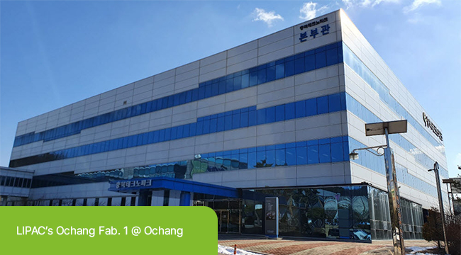
LIPAC's fabrication site is located at Ochang Scientific Industrial Complex in Chungcheongbuk-do, Republic of Korea, where IT convergence industry is vitalized at.

Address : Smart IT Kwan, Clean-room, 76, Yeongudanji-ro, Ochang-eup, Cheongwon-gu, Cheongju-si, Chungcheongbuk-do, Republic of Korea, 28116

For Inquiry

For more detailed information, please contact to info@LIPAC.co.kr

Terms of service

약관내용